In today’s microelectronic systems, where every facet can have an impact on the overall performance attained, the packaging employed is almost as important as the semiconductor dies themselves. Teledyne e2v Semiconductors fully appreciates this, and is in a position to offer the market its SiP and IC solutions in a wide range of different packaging formats.
A wealth of semiconductor packaging options
Packages can be non-hermetic or hermetically-sealed, depending on the nature of the applications they are intended for. Hermetically-sealed packages safeguard the die from potential damage via various sources (such as liquid or gas ingress, or the presence of contaminants). Likewise, packages can feature either organic or ceramic substrates.
Use of organic substrates will have benefits under certain circumstances, as the housing that encapsulates the die/dies will be thinner. The upshot of this is that more compact and low-profile solutions can be realized - saving board space and taking up less headroom. Conversely, ceramic-based packages that have been hermetically sealed are best suited to space deployments.
The hermetic aspect is highly effective at preventing potential issues caused by harsh environments. Ceramic substrates offer thermal properties that are more similar to those of the semiconductor die than organic ones. This can have benefits, as it prevents unwanted die flexing (and possible cracking) during heat fluctuations - thereby helping to increase long-term reliability.
Flip-chip capabilities
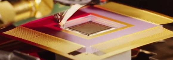
Packages can be flip-chip or have wire bonded die arrangements. Which is most appropriate will depend on the available room on the board, the I/O density and the cost constraints involved. This is where Teledyne e2v Semiconductors is, once again, able to stand out - since low-volume flip-chip solutions are incredibly difficult to find. There are very few vendors that have such capabilities and even those that do will generally only be able to deal with small-sized devices. Through the flip-chip capabilities that we can leverage, the automated processing of 300mm diameter wafers is supported. Die sizes of up to 560mm2 can be attended to, with as many as 10,000 bumps being incorporated at bump pitches going up to 150µm.